Introduction
Semiconductor manufacturing facilities in Singapore face some of the most demanding mechanical and electrical (M&E) engineering challenges of any building type. From floor slabs that must support equipment loads exceeding 50 kN/m² to chemical exhaust systems requiring 20 air changes per hour, the tolerances are razor-thin and the consequences of failure – contaminated wafers, regulatory shutdowns, or safety incidents – are severe. Successfully overcoming these M&E challenges requires specialized engineering design, strict regulatory compliance with Singapore authorities (BCA, SCDF, NEA, PUB), and systematic facility upgrade approaches tailored to the semiconductor sector.
This article covers the full spectrum of M&E engineering solutions for semiconductor manufacturing facilities in Singapore: heavy loading and structural design, chemical hazard management, precision environmental controls, authority submission processes, and practical upgrade strategies. It is written for facility managers, project developers, and engineering teams working on semiconductor manufacturing projects – whether greenfield fabs or upgrades to existing wafer fabrication parks.
Singapore’s semiconductor sector significantly contributes to its GDP, and the Singapore government committed S$18 billion for semiconductor R&D from 2021 to 2025 as part of broader government initiatives and initiatives aimed at strengthening the sector’s advanced manufacturing base. Nine of the top 15 semiconductor firms are already established in Singapore, making robust M&E engineering a competitive necessity for positioning Singapore as a global node in the semiconductor value chain, supporting global competitiveness and long-term economic growth.
By the end of this article, you will understand:
-
How to navigate regulatory approval processes with BCA, SCDF, and NEA for semiconductor facilities
-
Heavy loading solutions and structural system trade-offs for fab environments
-
Chemical hazard ventilation and containment requirements under Singapore’s codes
-
Precision environmental control strategies for tropical cleanroom operations
-
Cost-effective, systematic approaches to facility upgrades and commissioning
Understanding M&E Challenges in Semiconductor Manufacturing
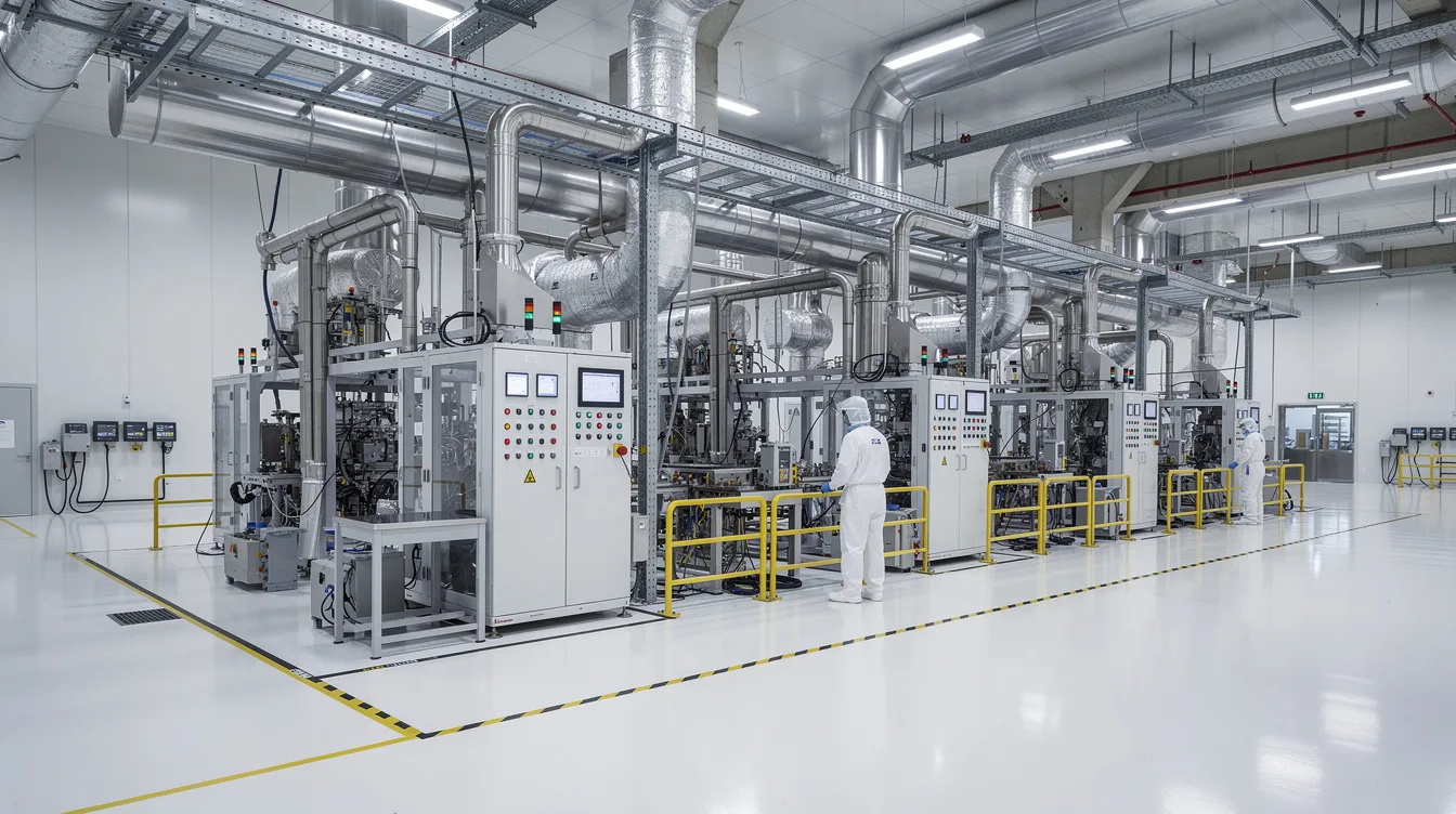
Mechanical and electrical engineering challenges in semiconductor manufacturing facilities differ fundamentally from those in commercial or even typical industrial buildings. Chip manufacturing demands simultaneous precision across multiple domains: structural systems must handle extreme point loads from fabrication tools, HVAC systems must maintain particle counts at ISO Class 3–5 levels, chemical distribution networks must safely deliver and exhaust hazardous process gases, and electrical infrastructure must guarantee uninterrupted power to prevent yield losses on every wafer.
In Singapore’s robust semiconductor ecosystem, these technical demands intersect with a dense regulatory environment, tropical climate conditions, and constrained urban land – creating a uniquely complex engineering landscape that the global semiconductor industry must address when operating here.
Heavy Loading and Structural Requirements in Wafer Fabrication
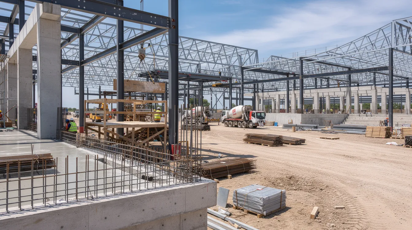
Heavy loading is one of the defining M&E challenges in semiconductor manufacturing facilities. Cleanroom tools – lithography systems, etch equipment, deposition chambers – generate massive static and dynamic point loads. Sub-fab infrastructure including vacuum pumps, abatement systems, and chemical delivery units adds further distributed loads across plenum levels. Air handling units (AHUs), chilled water piping networks, gas storage racks, and ceiling grid structures all impose loads that frequently exceed typical industrial building design assumptions.
Design loads for semiconductor equipment commonly exceed 20–50 kN/m² for point loads, with dynamic loads from vibration and moving components adding complexity. Singapore’s structural design codes, referencing SS EN 1990/1991 (adopted Eurocodes) and local BCA standards, require that all point load and live load calculations include worst-case dynamic scenarios. Foundation design is further complicated by Singapore’s coastal marine clay soils, which often necessitate piled foundations or thick reinforced slabs. BCA compliance for structural works in semiconductor facilities demands detailed PE-endorsed load analyses covering both current equipment and future tool replacement scenarios.
Chemical Hazard Management Systems
Semiconductor manufacturing processes use a wide range of hazardous chemicals – hydrofluoric acid, sulfuric acid, flammable solvents, toxic and pyrophoric gases – all requiring strict containment, storage, ventilation, and off-gas treatment. The M&E systems supporting chemical hazard management must be designed as independent, dedicated systems with built-in redundancy.
Under Singapore’s regulatory frameworks, the SCDF Fire Safety Code 2023 requires that rooms handling flammable or explosive substances have dedicated ventilation systems independent from office or support areas, with a minimum of 20 air changes per hour (ACH) and exhaust discharged to external space. Exhaust ducts passing through other compartments must be fire-rated. SS 641:2019 provides further detailed requirements for ventilation rates, fume hood performance, and containment in laboratory and chemical handling settings. NEA regulates the licensing and permitting for import, handling, storage, and discharge of chemicals, with SCDF having assumed control over seven formerly dual-regulated substances since 2020.
Precision Environmental Controls
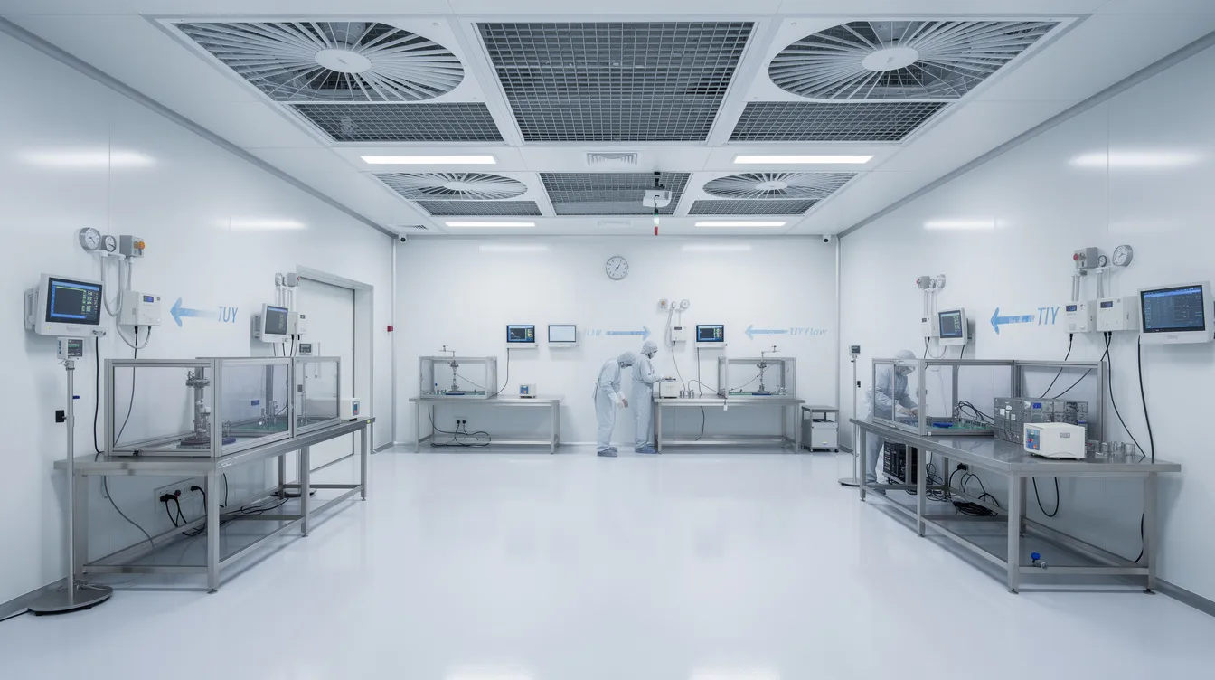
Cleanrooms in wafer fabrication facilities are classified under ISO 14644 (typically ISO Class 3–5), demanding extremely tight control of particle counts, differential pressures, temperature (often ±0.5 °C), humidity (±2% RH), and air velocity. The mechanical systems supporting these environments – ACMV units, HEPA/ULPA filtration, airflow balancing networks, and pressure cascade controls – represent the largest energy consumers in the facility, often requiring artificial intelligence for tighter environmental monitoring and control optimization.
Singapore’s updated standards SS 553:2026 and SS 554:2026 introduce revised climate design conditions reflecting higher outdoor humidity and wet bulb temperatures, directly impacting latent load calculations for semiconductor facilities. Dew point control is critical in Singapore’s tropical environment to prevent condensation, particle adhesion, and corrosion – all of which degrade manufacturing processes and equipment reliability while also supporting ongoing technological advancements in semiconductor production.
These foundational challenges set the stage for understanding how Singapore’s specific regulatory, climatic, and spatial conditions compound the engineering complexity of semiconductor manufacturing facilities.
Singapore Semiconductor Industry Association: M&E Implementation Challenges
Beyond the universal technical demands of semiconductor manufacturing, Singapore imposes a distinct set of implementation challenges rooted in its multi-agency regulatory structure, equatorial climate, and urban density. Understanding these factors early in the design process is essential to avoiding costly delays and redesigns.
Authority Submission Requirements
Semiconductor facility projects in Singapore require coordinated submissions to multiple statutory boards. BCA governs structural and building permit approvals, including buildability scoring and structural loading verification. SCDF handles fire safety plan approvals, hazardous substance licensing, and ventilation/exhaust system reviews for chemical handling areas. NEA manages environmental pollution control permits including chemical substance import, storage, and emissions discharge. PUB involvement is triggered when significant water supply or industrial wastewater systems are part of the scope.
Singapore’s semiconductor sector operates under rigorous regulatory frameworks. Missing documentation, mismatched standards (such as specifying international filter grades without confirming equivalency under Singapore’s codes), or insufficient detail on chemical safety duct routing will cause SCDF to reject submissions. For example, designs for air-handling units penetrating fire compartments must include fire dampers, proper compartmentation, and minimum separation distances between exhaust outlets and fresh air intakes. Scheduling pre-consultation meetings with each authority before formal submission is strongly recommended.
Tropical Climate Considerations
Singapore’s near-constant high temperature and humidity impose enormous cooling loads on semiconductor manufacturing facilities. Latent load control is critical – unmanaged moisture causes condensation on cold surfaces, promotes corrosion of ductwork and electrical components, and increases particle adhesion on wafer surfaces. Material selections must account for this: stainless steel ducts, corrosion-resistant coatings on structural steel, and sealed electrical enclosures are standard practice rather than optional upgrades.
Outdoor air intake for ACMV systems must be filtered and dehumidified before introduction to cleanroom support spaces. Singapore’s periodic haze events further complicate air quality management. SS 554:2026 mandates that during haze or elevated infection risk, filters treating outdoor or recirculated air must meet minimum efficiency of MERV14 (ASHRAE 52.2), F8 (EN 779), or ePM1 70–80% (ISO 16890-1). This requires HVAC systems designed with the flexibility to switch between normal and haze operating modes without disrupting cleanroom pressure cascades. Continuous monitoring of wastewater and emissions is essential for regulatory compliance in semiconductor production, adding another layer of environmental performance requirements.
Space Constraints and Urban Planning
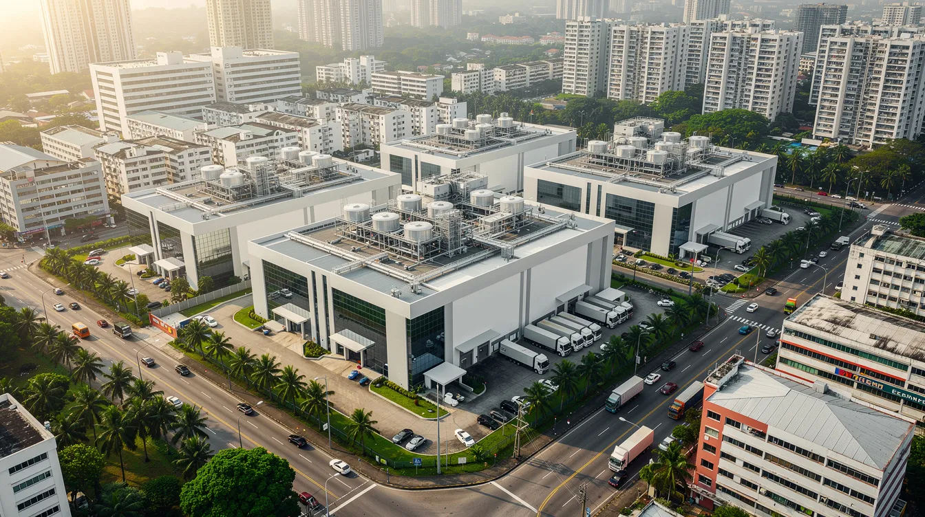
Industrial facilities like semiconductor fabs are typically sited in designated areas such as Jurong or Tampines, often on constrained footprints. Singapore is preparing 11% more land in wafer fabrication parks to meet increasing demand and accommodate global semiconductor firms, including semiconductor giants, but space efficiency remains paramount. Vertical stacking of cleanroom levels, plenum spaces, and sub-fab support floors is standard practice – but this creates conflicts between structural strength requirements, maintenance access, and ventilation routing.
URA’s development control handbooks specify minimum goods lift and loading bay requirements relative to gross floor area: buildings under 10,000 m² require 1 goods lift and 1 loading bay, 10,000–30,000 m² requires 2 each, and above 30,000 m² requires 3 each. Semiconductor fabs routinely exceed these thresholds and often need dedicated heavy-duty lifts to move fabrication tools weighing tens of tonnes. Space optimization strategies include shared infrastructure corridors, modular equipment layouts, and prefabricated MEP systems that reduce on-site assembly footprint.
These Singapore-specific constraints demand that M&E design teams move beyond standard engineering approaches and develop solutions calibrated to local conditions from the earliest project stages.
Detailed Engineering Solutions and Implementation
Moving from challenges to actionable solutions, this section outlines the systematic approaches that deliver reliable M&E performance in Singapore’s semiconductor manufacturing facilities.
Systematic Facility Upgrade Process
Facility upgrades are triggered by new tool installations, process technology changes, capacity expansions, responses to supply chain risks, or regulatory updates – all common in the fast-evolving global semiconductor landscape. A structured upgrade process prevents scope gaps and regulatory delays:
-
Conduct comprehensive M&E audit with PE endorsement – Assess structural capacity (floor loading, vibration profiles), HVAC system condition (filter integrity, airflow balancing, duct corrosion), power supply stability (transformer capacity, UPS health, generator readiness), and chemical handling safety (exhaust flow rates, containment integrity). Engage a qualified Professional Engineer to endorse findings.
-
Initiate authority pre-consultation – Present concept designs to BCA, SCDF, and NEA with clear documentation on structural loading, chemical safety, exhaust/intake routing, and redundancy. Obtain written feedback to align designs with current code requirements before committing to detailed engineering. This step alone can prevent months of approval delays.
-
Complete detailed M&E design – Select structural systems (reinforced concrete, steel frame, or hybrid) based on load, vibration, and construction speed requirements. Design cleanroom support spaces, chemical exhaust networks, HVAC systems, and power distribution with explicit compliance mapping to SS 553/554, SCDF Fire Code 2023, and SS 641. Integrated planning at this stage can reduce operational costs during later execution and compliance. Include filter specifications for both normal and haze operating modes.
-
Submit for full authority approval – File coordinated submissions to BCA (structural/building), SCDF (fire safety/chemical), NEA (environmental), and PUB (water/wastewater) with all test reports, material certifications, and standard equivalency documentation. Ensure M&E documentation is complete and cross-referenced.
-
Supervise construction and installation – Monitor structural works (floor slabs, steel beams, piled foundations), HVAC ductwork installation, electrical cable routing, and chemical storage/exhaust installations. Deploy prefabricated MEP modules where suitable to accelerate schedule, improve quality control, and help control operational costs.
-
Commission, test, and certify – Perform cleanroom testing per ISO 14644, airflow balancing verification, environmental parameter validation (temperature, RH, particle count, differential pressure), power reliability testing (including simulated voltage dip ride-through), and chemical exhaust flow rate confirmation. Engage third-party certification where required.
Real-time data integration improves monitoring accuracy in semiconductor fabs, and advanced AI and machine learning algorithms can predict equipment failures before they occur – making smart manufacturing principles increasingly important during the commissioning and operational phases.
Heavy Loading Solutions Comparison
Choosing the right structural system for a semiconductor facility involves balancing multiple performance criteria. The following comparison addresses the three primary approaches:
|
Criterion |
Reinforced Concrete |
Steel Frame |
Hybrid Systems |
|---|---|---|---|
|
Load Capacity |
Excellent – handles extreme static and dynamic point loads; ideal for heavy fab tools |
Good – suitable for distributed loads; may need additional floor mass for heavy point loads |
Very good – combines concrete slabs with steel framing for optimized load distribution |
|
Vibration Performance |
Superior natural damping – critical for lithography and precision tools sensitive to floorborne vibration |
Lower inherent damping – requires supplementary vibration isolators or floating floor systems |
Good – concrete floor slabs provide damping while steel allows long spans |
|
Installation Speed |
Slow – requires extensive formwork, curing time, and sequential construction |
Fast – prefabricated steel components enable rapid erection and easier modification |
Moderate – balances concrete pour schedules with steel erection speed |
|
Cost Efficiency |
Higher upfront cost; lower long-term maintenance in corrosive environments |
Lower initial cost; higher maintenance due to corrosion protection needs in tropical humidity |
Moderate cost; optimizes material usage by applying each system where most effective |
|
Fire Resistance |
Inherent fire resistance – no additional fireproofing required for structural elements |
Requires applied fireproofing (intumescent coatings, board systems) |
Mixed – concrete elements provide inherent resistance; steel components need protection |
|
Service Routing Flexibility |
Limited – penetrations through concrete require advance planning and structural verification |
Excellent – open steel framing accommodates complex M&E routing and future modifications |
Good – steel sections facilitate routing while concrete provides structural mass |
For most semiconductor manufacturing facilities in Singapore, hybrid systems offer the best overall balance: reinforced concrete slabs and foundations provide the mass, damping, and fire resistance that precision semiconductor equipment demands, while steel framing above allows construction speed, routing flexibility, and easier future modifications. The choice should be validated through parametric vibration studies during early design – especially for advanced node fabs where lithography tools have sub-nanometre positioning requirements.
A notable benchmark: Johnson Controls delivered a 24,000 sqm cleanroom for a greenfield fab project in Singapore in just 18 months, demonstrating that integrated engineering approaches with pre-engineered and modular components can achieve both structural performance and aggressive schedules.
Common Supply Chain Challenges and Solutions
Even well-designed semiconductor manufacturing facilities encounter recurring M&E issues during construction, commissioning, and operation. The following represent the most frequently encountered problems in Singapore fab projects and their proven solutions.
Regulatory Approval Delays
Regulatory approval delays are the single most common source of schedule overruns in semiconductor facility projects. They typically stem from incomplete submissions – missing structural load analyses, unconfirmed filter equivalencies under Singapore codes, insufficient chemical safety documentation, or fire-rated construction details that fail to address SCDF Fire Code 2023 requirements for compartmentation, fire dampers, and exhaust/intake separation distances (minimum 5 m).
Solution: Engage experienced M&E consultants who have prior approval track records with BCA, SCDF, and NEA for semiconductor and high-tech facilities. Schedule formal pre-consultation meetings with each authority before detailed design begins. Use precedent drawings and mock-up submissions to identify potential rejection points early. The Economic Development Board and Enterprise Singapore can also facilitate introductions and guidance for multinational corporations establishing semiconductor manufacturing bases in Singapore.
Chemical Ventilation System Failures
Chemical ventilation failures in semiconductor facilities typically result from undersized exhaust systems, single points of failure in fan or ductwork configurations, inadequate fire rating of exhaust ducts, or insufficient separation between exhaust discharge points and fresh air intakes. In Singapore’s humid climate, corrosion accelerates duct degradation if materials are poorly specified.
Solution: Design dedicated exhaust systems with N+1 redundancy for all chemical handling areas. Specify fire-rated ducts for any exhaust shaft passing through fire compartments. Install chemical sensors and automatic interlocks that trigger emergency ventilation modes. Ensure exhaust-to-intake separation meets the minimum distances specified in SCDF Fire Code 2023 Clause 7.1. Implement rigorous maintenance protocols with scheduled duct inspections and corrosion monitoring, especially for systems handling corrosive fume exhaust. Monitoring and evaluation in semiconductor manufacturing encompasses process control and quality assurance – extending this discipline to ventilation systems prevents degradation from going undetected.
Equipment Vibration and Interference
Precision semiconductor equipment – particularly lithography systems, metrology tools, and inspection equipment – is extremely sensitive to vibration. Floorborne vibration from nearby mechanical equipment (fans, pumps, compressors), foot traffic, or external sources (road traffic, construction) can compromise nanometre-scale process accuracy. Acoustic noise from HVAC systems can couple into structural vibration paths.
Solution: Conduct parametric vibration studies during early structural design to identify critical frequency ranges. Implement floating floor systems or isolated equipment pads with tuned dampers for vibration-sensitive tools. Isolate all M&E equipment (fans, pumps, chillers) with spring mounts or inertial bases. Separate vibration-sensitive production areas from mechanical plant rooms using structural breaks. Specify vibration criteria (typically VC-D or VC-E for advanced lithography) and verify compliance during commissioning with instrumented measurements.
Power Supply Stability Issues
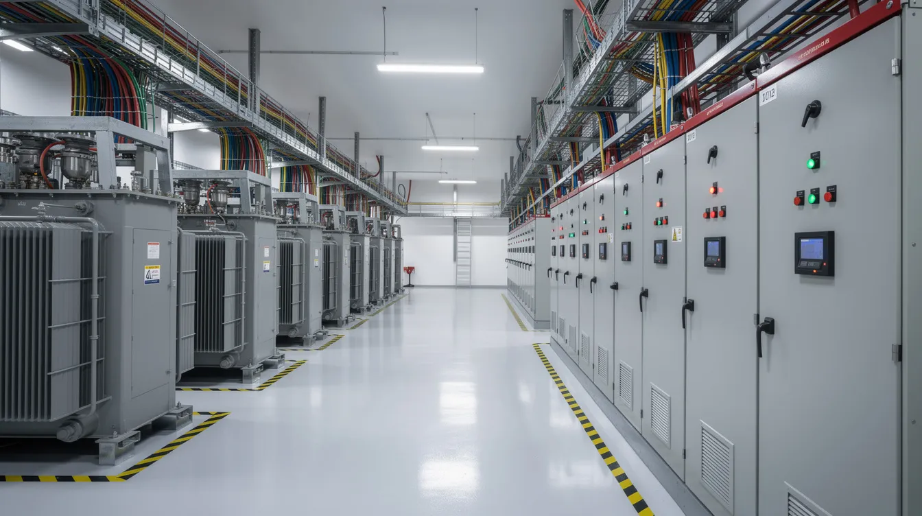
Semiconductor manufacturing facilities are uniquely vulnerable to power quality issues. Even a two-second voltage dip can destroy an entire batch of wafers in process, representing losses of potentially millions of dollars. Harmonics from variable-frequency drives and non-linear loads degrade power quality across the facility. Singapore’s electrical grid is reliable, but fab-internal distribution must be engineered for absolute continuity.
Solution: Size transformers with adequate margin for current and future tool loads. Micron Technology’s planned Singapore fab is reported to need 400–500 transformers – more than double the typical fab requirement – highlighting that heavy electrical infrastructure is becoming a critical bottleneck as semiconductor technologies advance. Implement redundant utility feeds (N+1 or 2N depending on criticality), UPS systems with sufficient hold-up time to bridge generator startup, and active harmonic filters on all major non-linear loads. Test power ride-through capability under simulated worst-case voltage dip scenarios during commissioning. OEMs now maintain higher-than-normal chip inventories post-pandemic, intensifying the pressure on fabs to maintain uninterrupted production and avoid supply chain vulnerabilities.
A systematic approach to these common challenges – grounded in Singapore’s specific regulatory codes, climate conditions, and operational demands – is what separates successful semiconductor facility projects from those plagued by delays and performance shortfalls.
Conclusion and Next Steps
Overcoming M&E challenges in high-tech semiconductor manufacturing facilities in Singapore requires a comprehensive engineering approach that integrates structural design for heavy and dynamic loads, chemical hazard management compliant with SCDF and NEA requirements, precision environmental controls calibrated for tropical conditions, and electrical infrastructure engineered for absolute reliability. The complexity is compounded by Singapore’s multi-agency regulatory environment and the increasing demands of advanced semiconductor technologies – but these challenges are manageable with the right expertise and methodology.
Singapore’s semiconductor ecosystem includes nine of the top 15 global firms, and with the Singapore government having committed S$18 billion for semiconductor R&D from 2021 to 2025, investment in world class infrastructure is accelerating. A*STAR launched the world’s first 200mm Silicon Carbide Open R&D Line, and the Lab-in-Fab program reduces time-to-market for semiconductor prototypes that enable next-generation applications such as electric vehicles – reflecting the continuous technological innovation driving innovation across the semiconductor industry. The Singapore Semiconductor Industry Association collaborates with educational institutions, including a leading national university, for talent development, while specialised training and internships strengthen the local workforce and address talent shortages in the sector. Collaboration with local educational institutions can enhance talent pipelines, and Singapore emphasizes workforce capability development to address skilled engineer shortages – because even the best-designed facilities require a skilled workforce to operate and maintain them. Singapore ranked #2 globally in the International Property Rights Index 2024, reinforcing the strong governance framework that underpins the nation’s competitive edge in the global semiconductor landscape.
A*STAR’s initiatives nurture local expertise and attract international talent, supporting the strategic partnerships and industry academia collaborations that semiconductor innovation demands. Government offers tax breaks and grants to attract semiconductor companies and support innovation, while Singapore plans to expand wafer fabrication parks by 11% for semiconductor firms – signalling sustained commitment to the sector’s growth.
To move forward on your semiconductor facility project, take these immediate steps:
-
Conduct a comprehensive facility assessment – Engage a qualified PE to audit structural capacity, HVAC performance, power infrastructure, and chemical handling systems against current code requirements
-
Engage qualified M&E consultants with specific semiconductor facility experience – look for demonstrated track records with BCA, SCDF, and NEA submissions for high-tech manufacturing environments
-
Initiate pre-submission consultations with all relevant authorities before committing to detailed design – this single step prevents the most common cause of project delays
For teams planning future expansions, ongoing maintenance protocol development, emerging semiconductor technology requirements (including advanced packaging and next-generation semiconductor equipment), and energy efficiency optimization under NEA’s industrial energy roadmap are critical areas for continued focus. Environmental performance is now a key aspect of semiconductor manufacturing monitoring, and the trend toward smart manufacturing with real-time data integration and machine learning will continue reshaping how facilities are designed, operated, and maintained. A*STAR announced three initiatives to enhance semiconductor innovation, further positioning Singapore as a centre of technological leadership in Southeast Asia and across the global semiconductor value chain.
Additional Resources
-
Singapore regulatory authorities: BCA for building control and structural standards, SCDF Fire Code 2023 for fire safety and chemical ventilation requirements, and NEA for environmental licensing and energy efficiency roadmaps that also support semiconductor capacity serving end-use markets such as mobile phones
-
Professional engineering consultation: M&E engineering compliance guidance for navigating Singapore’s multi-agency approval processes, and comprehensive M&E consultancy services for semiconductor facility projects
-
Industry standards: SS 553:2026 and SS 554:2026 for ACMV and indoor air quality, SS 641:2019 for laboratory chemical safety, ISO 14644 for cleanroom classification and testing, and BCA’s prefabricated MEP system guidelines for modular construction approaches